Before the lab

Purpose and workflow

Your objective

Use a BC547 NPN transistor as an inverting switch, measure its voltage-transfer characteristic (VTC), and measure its switching response time.

Build

Construct and check two transistor-switching circuits.

Measure

Capture static transfer and dynamic timing behaviour.

Explain

Connect cutoff, transition, and saturation to digital inversion.

Bring and locate

Components and leadsBench equipment
Breadboard, jumper wires, banana leads, alligator clips, BNC-to-alligator lead, BNC-to-probe leadABRA AB-3300 DC supply, GW INSTEK GFG-8216A function generator, RIGOL DS1052E oscilloscope, BK Precision 2831D DMM
BC547 NPN transistor; one red and one green LED; two 390 Ω, one 220 Ω, and one 1 kΩ resistorInstructor-approved component information and the circuit figures below

Safety first

Make the bench safe before wiring

Power off before changes.

Disconnect the DC supply and function generator before inserting, removing, or moving any wire or component. Your instructor must check each newly built circuit before you apply power.

  1. Wear closed-toe shoes and safety glasses; remove dangling metal or jewellery. Know the exits, emergency power shutoff, and extinguisher location.
  2. Keep the bench clear. Do not open or relocate equipment. Do not use damaged leads or instruments; report them.
  3. Check LED polarity and the exact BC547 pinout before insertion. Avoid touching component leads unnecessarily.
  4. Use a common circuit reference: DC supply ground, function-generator ground, and oscilloscope probe grounds must connect to the circuit ground shown. Never clip a grounded scope lead to an arbitrary powered node.
  5. Avoid shorts and stay within component ratings. If anything heats, smells, or smokes, turn off supplies, disconnect sources, and tell the instructor.

Need a refresher?
→ Basic Laboratory Safety

Configure sources while disconnected

DC supply

Use an adjustable protected output—not the fixed 5 V/3 A terminals. Set independent mode, 5 V, and a current limit near 100–200 mA. Begin at the lowest current and raise it only until constant-current indication stops. Verify voltage with the DMM.

Function generator

Select the required waveform, frequency range, amplitude, and offset while disconnected. Verify the actual signal on the oscilloscope before attaching it to the transistor circuit.

Preparation

Identify parts before insertion

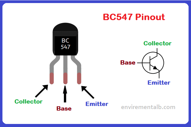
BC547 flat-face package drawing labelled collector, base, and emitter from left to right
BC547 transistor pin identification. Verify the marking and datasheet for your exact part.
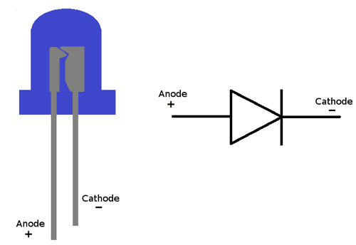
LED drawing showing the longer anode lead and shorter cathode lead beside the flat package edge
LED polarity cues: longer lead is usually the anode; the flat edge is nearest the cathode.
Do not assume all NPN packages share a pin order.

Read the marking on your transistor, find the approved datasheet for that exact part, and confirm collector, base, and emitter. For the BC547 shown here, the flat face toward you is C–B–E from left to right; verify the installed part before wiring.

PartCheck before use
390 Ω ×2, 220 Ω, 1 kΩRead the colour code or measure resistance; use ¼ W parts and remain below their rating.
Red and green LEDsIdentify anode/cathode; a series resistor is mandatory.
BC547Record the full marking and confirm C, B, E from approved component information.
BreadboardTrace connected rows and separated power rails with power off.

Need refreshers?
→ Breadboard Fundamentals · → Convert resistor colour bands to a resistance value · → BC547 Reference

Experiment 1

LED transistor switching circuit

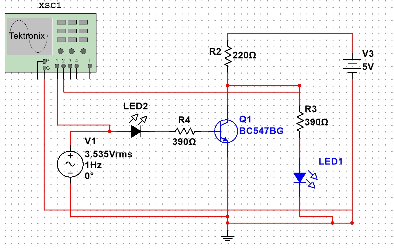
LED transistor switching circuit with a 5 volt supply, BC547 transistor, LEDs, 220 ohm collector resistor, and 390 ohm resistors
LED transistor switching circuit. LED1 is red and LED2 is green. Use the labelled component values and verify Q1 terminals before wiring.
Generator settings

Set a sine wave at 5 V peak-to-peak, 0 V DC offset, and 1 Hz. Verify all three settings directly on the oscilloscope before connection.

  1. Power off: build the circuit exactly as shown. Join all source and instrument grounds at circuit ground.
  2. Connect oscilloscope Channel 1 to the function-generator input node and Channel 2 to the transistor output/collector node. Set each probe attenuation correctly in both probe and scope menus.
  3. Configure and verify the generator while disconnected: sine, 5 Vpp, 0 V offset, 1 Hz.
  4. Ask the instructor to inspect the wiring. Then apply 5 V DC and the verified input.
  5. Display one or two complete cycles. Use Measure or the graticule to obtain input period and peak-to-peak voltage. Observe both LEDs over several cycles.

Need refreshers?
→ Using a Function Generator · → Using an Oscilloscope

Experiment 2 · static

Measure the voltage-transfer characteristic

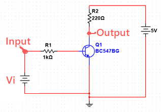
Common-emitter BC547 circuit with input through 1 kilohm base resistor, emitter grounded, and collector output pulled to 5 volts through 220 ohms
Simple transistor switching circuit used for the VTC and timing work.
  1. Power off and replace the LED circuit with the simple circuit shown. Ask the instructor to check it before applying power.
  2. Use the DMM to measure actual input voltage Vi and output voltage Vo.
  3. Starting at 0.0 V, adjust the DC input through 5.0 V in 0.1 V setpoint steps. At every step, record the actual input and output. Approach each setting deliberately; do not rewire live.
  4. Plot Vo versus Vi in Excel. Label axes and units and use a scatter plot that preserves numeric spacing.
  5. From the plot, estimate VOHVmax and VOLVmin. Find VM where the curve meets Vo=Vi; draw the tangent at that point and extend it to the high and low output levels to estimate VIL and VIH.

Need refreshers?
→ Using a Digital Multimeter · → Voltage Transfer Characteristic

VTC measurements

Sweep Vi from 0.0 V to 5.0 V in 0.1 V increments. At each step, record the actual Vi and measured Vo in volts.

Target inputActual Vi (V)Vo (V)

Experiment 2 · dynamic

Measure switching response time

  1. Keep the simple transistor circuit. With its input disconnected, configure a square wave at 5 Vpp, 0 V offset, and 1 kHz; verify it on the oscilloscope.
  2. Connect Channel 1 to Vi and Channel 2 to Vo. Use a shared ground and display both traces.
  3. Increase frequency until the output rise and fall intervals are clearly visible. Adjust time/div and volts/div without hiding either transition.
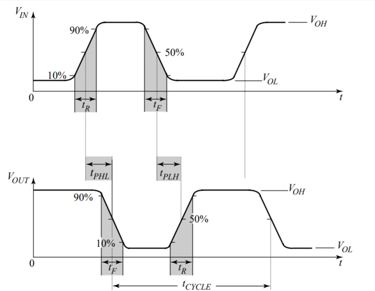
  4. Measure output rise time tR, fall time tF, high-to-low propagation delay tPHL, and low-to-high propagation delay tPLH using consistent threshold points.
  5. Save a scope snapshot that shows both signals, scales, and the transitions used.
Timing diagram with input and inverted output waveforms, showing propagation delays plus output rise and fall intervals
Switching-time measurement definitions for propagation delay, rise time, and fall time.

Need a refresher?
→ Rise, Fall, and Propagation Time

MeasurementValueUnit
Rise time, tR
Fall time, tF
High-to-low delay, tPHL
Low-to-high delay, tPLH

Analysis

Think it through

Answer from your own circuit, plots, and waveforms. Explain relationships rather than restating measurements.

Completion

Review and create the local submission ZIP

Keep the actions distinct

Completing this manual saves responses in this browser. Selecting evidence adds live files to the next locally generated ZIP. Neither action uploads to Avenue. Follow your instructor’s current direction for submission.

  • Confirm the instructor checked circuits before power and discussed your alternate VTC method.
  • Confirm the three evidence files clearly show the requested milestone.
  • Download the ZIP in this same session; after reload, evidence files must be reselected.

Submission package

Download your Lab 1 submission ZIP

The ZIP includes completion.json and the evidence files selected in this browser session.

Submission Details

Enter all four required details before downloading: Student Names, Student Numbers, Lab Section, and Lab Instructor.

Evidence files must be reselected after reopening the page.