Implement, program, and verify combinational logic with a DE0-Nano FPGA.
Quartus Prime 25.1 LiteEP4CE22F17C6DE0-Nano FPGA
Orientation
From logic gates to configured hardware
Objectives
Use Quartus Prime 25.1 Lite and a DE0-Nano board to create schematic and Verilog combinational designs, compile them, assign pins, program the FPGA, and verify behaviour with switches and LEDs.
Schematic design
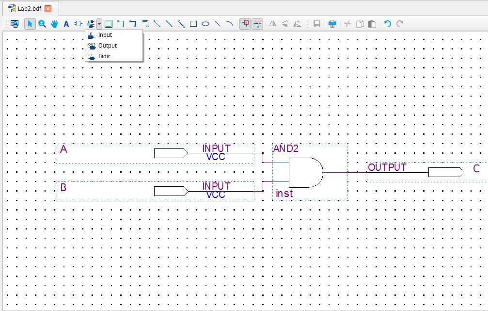
Build logic graphically with a Block Diagram/Schematic File.
Verilog design
Describe hardware with Verilog HDL.
Both paths
Compile, assign I/O, program, and test the actual board.
Equipment
Learn the DE0-Nano board
Before you build anything, use the DE0-Nano board guide to find the basic board information below. You do not need to memorize it. Open the guide, find each answer, and type it into the matching box.
Safety first. Keep the board on a non-conductive surface. Turn power off before moving wires. Only program the board after the USB-Blaster and board connection are secure.
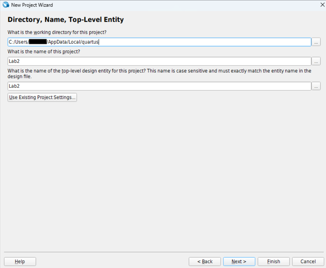
Choose File → New Project Wizard. Create a writable project folder; use a short project name and use the same top-level entity name for the first design.
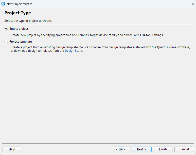
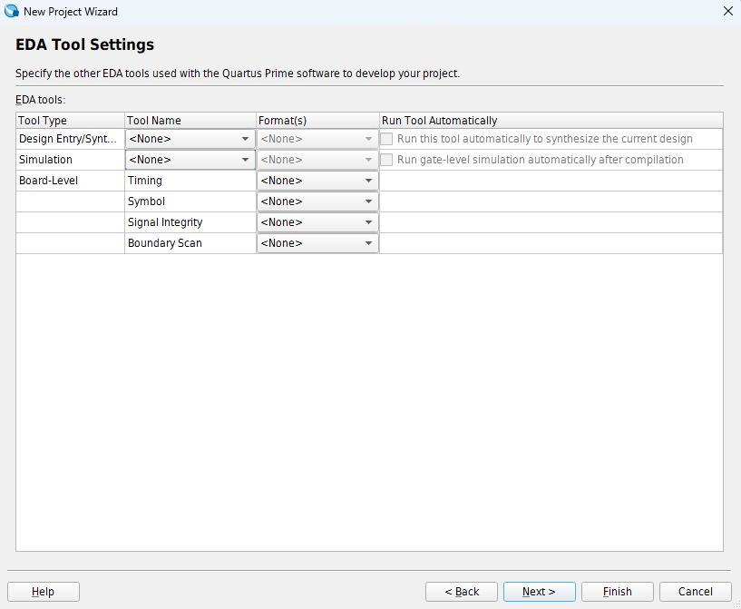
Select Empty project; do not add files yet.
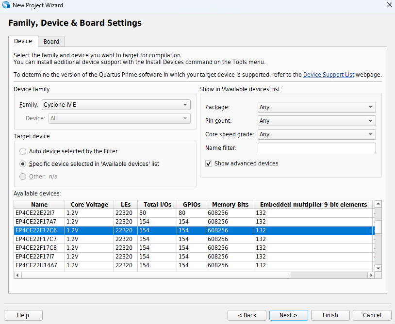
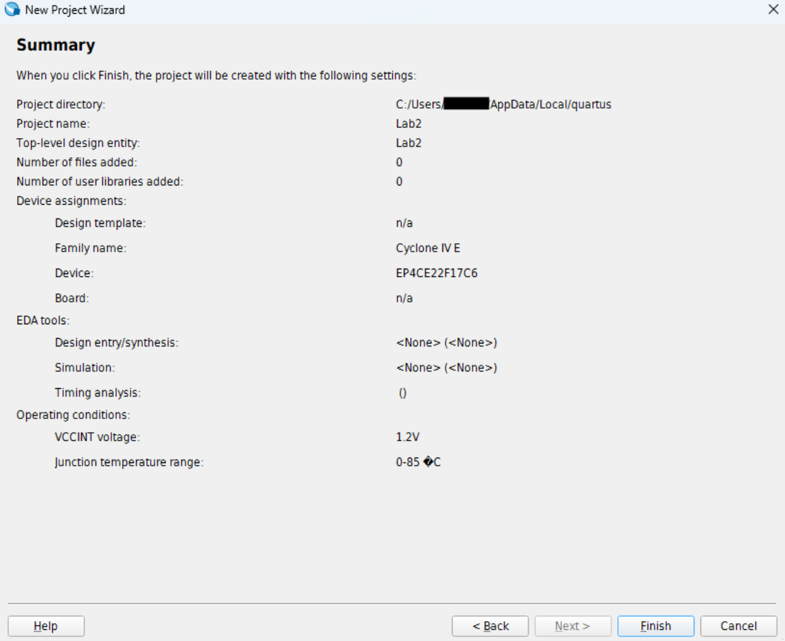
Select the Cyclone IV E target device EP4CE22F17C6. Review the project summary and finish.
Save the project before creating a design file.
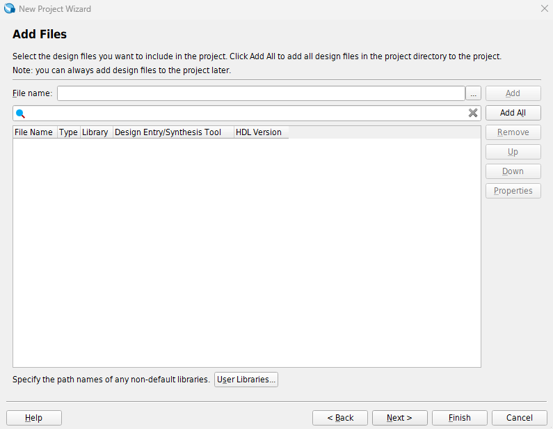
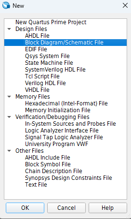
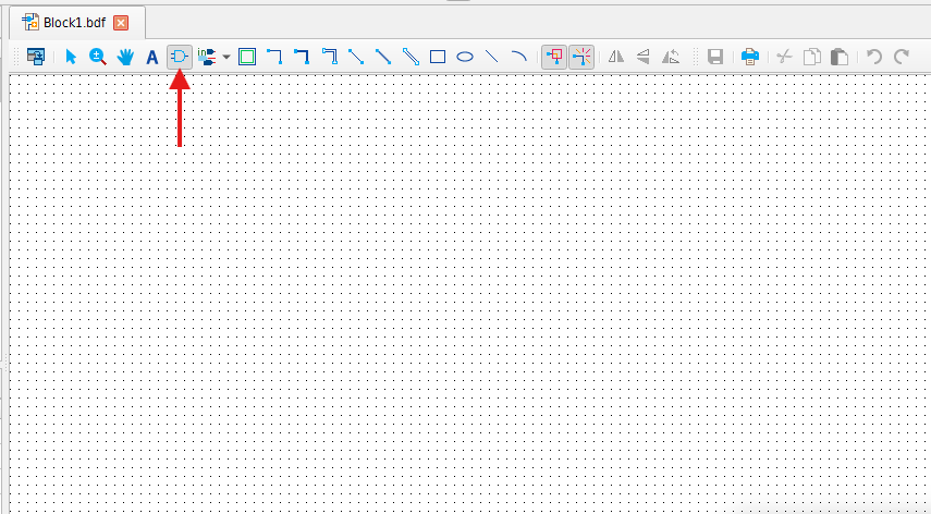
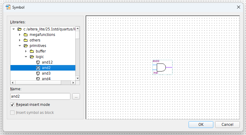
Enter a project folder, project name, and matching top-level entity name.Choose Empty project.Do not add design files yet; click Next.Select the Cyclone IV E device EP4CE22F17C6.Leave the EDA tool settings at their defaults.Check the summary, then click Finish.Later, use File → New to create a Block Diagram/Schematic File.
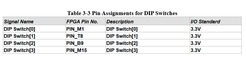
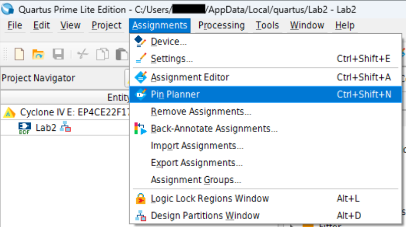
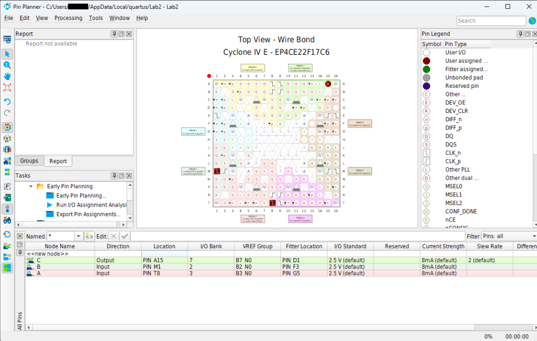
Open Assignments → Pin Planner. Assign the input and output ports to the required DE0-Nano switch and LED pins. Confirm each assignment against the board reference.
Save, then compile again so the assignment changes are included.
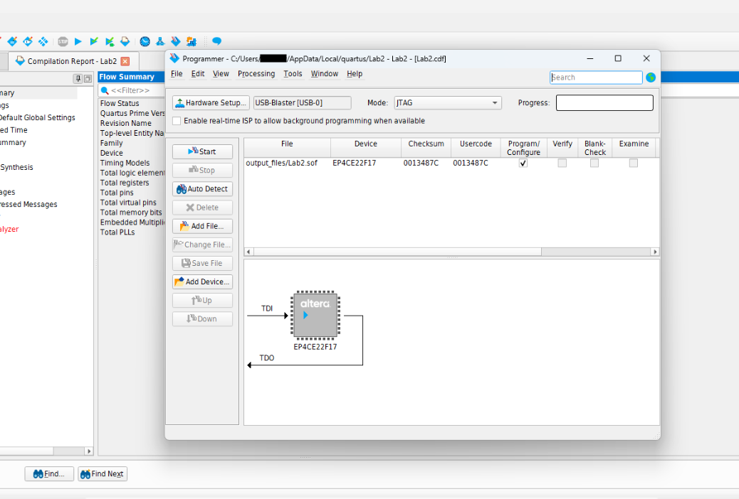
Open Tools → Programmer. Select USB-Blaster, use JTAG mode, and add the compiled .sof from output_files.
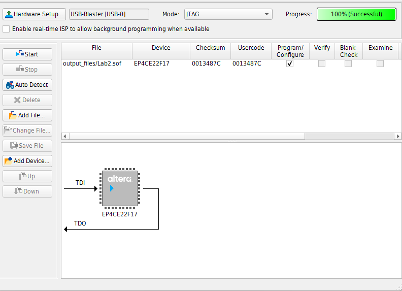
Start programming. The .sof is the compiled SRAM configuration file loaded into the FPGA for the current design.
Test all A/B combinations using the assigned DIP switches and LED output. Show the working AND gate to the instructor.
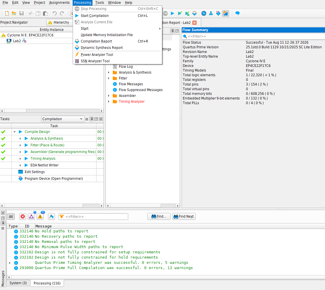
Compile the project and confirm that the compile completes successfully.Use the board reference for the DIP-switch pin assignments.Open Assignments → Pin Planner.Enter and check the pin locations for A, B, and the output.Open Programmer, choose USB-Blaster and JTAG, and add the compiled .sof.Click Start and wait for the successful programming result.
Logic gates
Implement and verify logic gates
Create and test OR, NAND, NOR, XOR, and XNOR using the same project flow. Replace the primitive, save, compile, assign pins if needed, program the FPGA, and test every DIP-switch combination. Enter the predicted output and your LED observation.
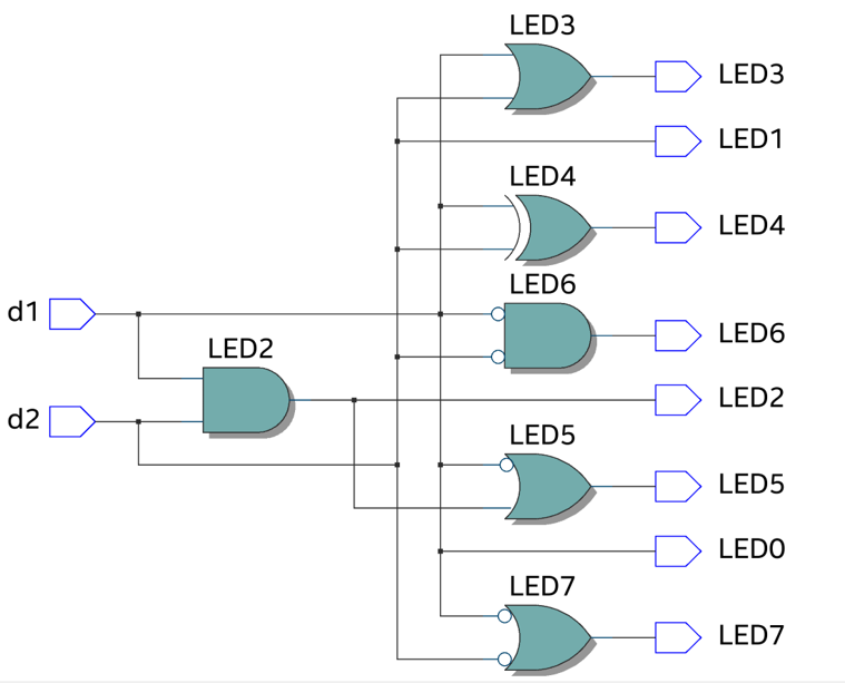
Build and test the supplied combinational circuit. Keep the signal names and LED output labels exactly as shown.
Using the supplied circuit diagram, analyse the function, build the complete schematic, compile it, assign the required I/O, program the FPGA, and verify the output combinations on the board. Do not simplify the circuit until you have recorded its required behaviour.
Verilog HDL
Describe combinational hardware with Verilog
A schematic describes hardware graphically. Synthesizable Verilog describes the intended hardware with modules, ports, and logic expressions; synthesis converts that description into FPGA logic.
Create File → New → Verilog HDL File, then save it with the file name of your choice.
Define one module whose name matches with your file name. Declare its inputs and outputs, then implement the specified combinational behaviour.
Add the saved file to the project and confirm it appears in project files. Save all.
Run Analysis & Synthesis, correct syntax errors, and confirm the top-level entity is correct.
Type or paste this starter code into your Verilog HDL file. The file name and top-level module must match your file name.
Build and test
Compile the design and test the board
Now turn your Verilog file into a working FPGA program. Follow these steps in order.
In Quartus, run Analysis & Synthesis. Then choose Tools → Netlist Viewers → RTL Viewer.
Take a screenshot of the RTL Viewer. This shows the logic Quartus found in your Verilog file.
Open Pin Planner. Enter the LED and switch pin numbers, save, and compile the project again.
Open Programmer, select USB-Blaster, load the new .sof file, and click Start. Test the LEDs and switches on the board.
Analysis
Think it through
Completion
Review and create the local submission ZIP
Demonstrate the completed laboratory work and your programming checklist to the instructor. The ZIP retains the required responses and files selected in this browser session.
Submission package
Download your Lab 2 submission ZIP
The ZIP includes completion.json and selected evidence/design files.
Submission Details
Enter all four required details before downloading.
Evidence files must be reselected after reopening the page.